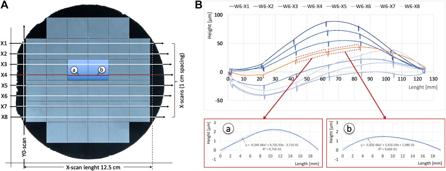
Wafer-Level Component Measurements

Frontiers Wafer Level Packaging Technology Applied to Pixel Detectors
Wafer-Level Component Measurements
Understanding Wafer Level Packaging - AnySilicon
MEMS integration using wafer-level packaging - CMM Web Portal
Panel Process for Fan Out Wafer Level Packaging: Part Four, Build-Up Films for Redistribution Layers (RDL) - Polymer Innovation Blog
Frontiers Wafer Level Packaging Technology Applied to Pixel Detectors
Polymers in Electronic Packaging: Introduction to Fan-Out Wafer Level Packaging - Polymer Innovation Blog

Novel Opto-Electronical Probe Card for Wafer-Level PIC Testing
Wafer Chip Size Package (WLP) Dummy Component
Sie können auch mögen

Schlagen Sie Suchanfragen


