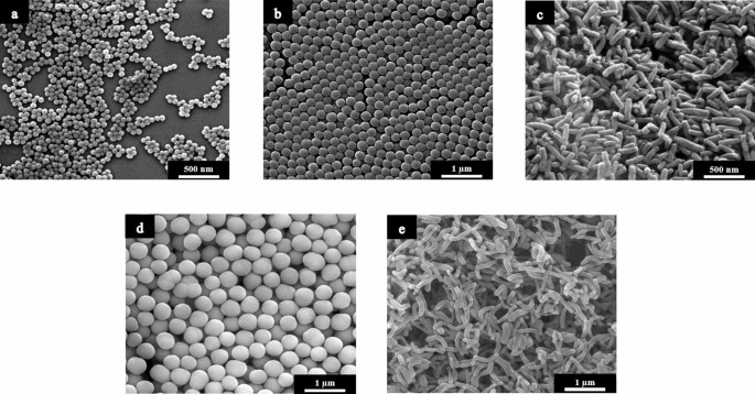
a) SEM image of crystallized silica spheres on a plain Si substrate.

Download scientific diagram | (a) SEM image of crystallized silica spheres on a plain Si substrate. The small black and large white squares represent the areas used for the calculation of the Fourier transforms in Figure 3c and d. (b) Optical micrograph of the etched substrate after the crystallization of silica opals (about 1 mm × 0.7 mm). The high-lying parts of the wafer are uncovered (blank silicon ) white); the low-lying etched pattern is completely filled (dark). (c, d) Representative SEM images showing the same selectivity. Notice the difference between isolated trenches and trenches of the same size, which are connected to a continuous trench in part d. from publication: Integration of Self-Assembled Three-Dimensional Photonic Crystals onto Structured Silicon Wafers | We report on the fabrication of high-quality opaline photonic crystals from large silica spheres (diameter of 890 nm), self-assembled in hydrophilic trenches of silicon wafers by using a novel technique coined a combination of "lifting and stirring". The achievements reported | Silicon Wafer, Photonic Crystals and Self-Assembly | ResearchGate, the professional network for scientists.

SEM Images of silica

In situ cracking of silica beads in the SEM and TEM — Effect of particle size on structure–property correlations - ScienceDirect

SEM images of varied morphology of microscopic-scale spheres
Optical transmission and laser structuring of silicon membranes

Dip Coating Passivation of Crystalline Silicon by Lewis Acids
Optical transmission and laser structuring of silicon membranes

Amorphous silicon from low-temperature reduction of silica in the molten salts and its lithium-storage performance - ScienceDirect

Sustainable Encapsulation Strategy of Silicon Nanoparticles in Microcarbon Sphere for High-Performance Lithium-Ion Battery Anode
Subtoxic cell responses to silica particles with different size and shape